How to Choose a Prototype Circuit Board in 2026?
Choosing a Prototype Circuit Board in 2026 requires more than comparing board prices. A design may look simple on a screen, yet fail after assembly. A 1.6 mm FR-4 board can struggle with heat, impedance, or connector stress. Small decisions matter.
Prismark’s 2024 PCB Industry Results and 2025 Outlook highlights continued demand from artificial intelligence infrastructure, automotive electronics, and high-performance computing. These applications raise expectations for layer count, signal integrity, thermal management, and manufacturing consistency. IPC market reports also show why delivery time and supply stability deserve attention, not only unit cost. A delayed prototype can postpone firmware testing, regulatory preparation, and customer feedback.
Mike Buetow, president of the Printed Circuit Engineering Association and a longtime PCB industry analyst, has said, “The printed circuit board is the foundation of all electronics.” That foundation must match the product’s real operating conditions. A practical selection process should examine material type, copper weight, layer structure, controlled impedance, surface finish, via technology, and assembly capability. Ask whether the supplier can review Gerber files, inspect solder joints, and document electrical tests. Evidence matters.
Cheap is not always economical.
A two-layer board may suit a sensor, but it can become a poor choice for a fast processor. A four-layer Prototype Circuit Board may cost more initially, while reducing noise and rework. IPC-2221 and IPC-A-600 provide useful design and acceptance guidance, but no standard replaces engineering judgment. The best decision remains partly imperfect. Prototype quantities are small, data can be incomplete, and assumptions deserve testing before production.
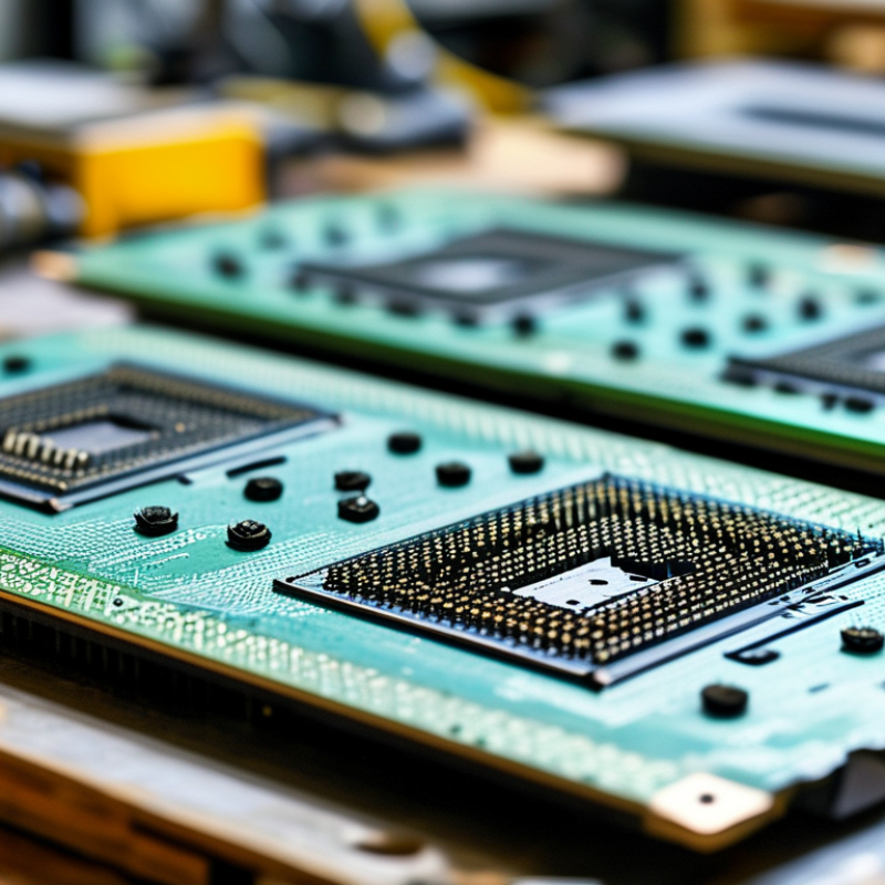
Define the Prototype’s Electrical and Mechanical Requirements
How to Choose a Prototype Circuit Board in 2026?
Define the Prototype’s Electrical and Mechanical Requirements
A reliable prototype begins with measurable electrical requirements. Record voltage range, current draw, signal frequency, and expected operating temperature. Separate normal values from temporary peaks. A board that passes a desk test may fail inside a warm enclosure. I have seen early designs overlook connector losses and cable resistance. Those small details changed the power budget.
Mechanical requirements deserve equal attention. Measure the enclosure’s internal space, mounting points, board thickness, and access clearances. Mark the position of buttons, displays, sensors, and cables. Check whether the board needs to survive vibration, repeated handling, or moisture exposure. Do not assume standard dimensions will fit. That assumption is often wrong. Leave room for probing, component replacement, and airflow around heat-producing parts.
Tips: Create a one-page requirement sheet before selecting the board. Include tolerances, not only target values. Use a multimeter and oscilloscope to verify real loads during testing. Compare the prototype’s connector locations with a simple enclosure mock-up. Paper can reveal interference early. Also record every design change. A forgotten revision can make test results unreliable. When requirements remain uncertain, choose a flexible board layout and label unverified assumptions clearly. This may increase short-term work, but it reduces expensive redesigns later.
How to Choose a Prototype Circuit Board in 2026? - Define the Prototype’s Electrical and Mechanical Requirements
| Requirement | Typical Prototype Range | Recommended Board Consideration | Why It Matters | Selection Check |
|---|---|---|---|---|
| Supply voltage | 3.3 V, 5 V, 12 V, or multiple rails | Use a board and connector system rated above the maximum continuous voltage; provide separate power and signal routing where required. | Voltage margin reduces insulation stress and improves safety during laboratory testing. | Confirm maximum operating voltage, transient voltage, polarity, and required creepage distance. |
| Continuous current | Signal circuits: <100 mA; small power paths: 0.5–3 A | Choose wider copper traces, heavier copper, reinforced terminals, or dedicated power planes for higher current. | Trace resistance produces voltage drop and heat; allowable current depends on copper thickness, width, and temperature rise. | Calculate trace width from current, copper thickness, allowable temperature rise, and conductor length. |
| Digital signal speed | GPIO to approximately 10–50 MHz; faster buses require controlled layout | For fast edges or high-speed interfaces, use a multilayer board with a continuous reference plane and short return paths. | Signal integrity is determined by edge rise time, trace geometry, impedance, and return-current behavior—not only clock frequency. | List interface type, estimated rise time, maximum trace length, impedance target, and termination method. |
| Analog and mixed-signal performance | Millivolt-level signals, sensor inputs, and 12–24-bit data conversion | Use separated analog and digital regions, a low-impedance ground strategy, short sensor paths, and adequate decoupling. | Digital switching noise, ground impedance, and power-supply ripple can reduce measurement accuracy. | Define noise limit, bandwidth, resolution, sampling rate, reference voltage, and grounding method. |
| RF or wireless operation | Approximately 100 MHz to 6 GHz for common prototype work | Prefer a stable dielectric construction, controlled-impedance transmission lines, continuous ground planes, and a defined antenna keep-out area. | Dielectric variation, discontinuities, vias, and nearby metal can change impedance and antenna performance. | Specify operating band, 50 Ω interfaces where applicable, antenna location, enclosure material, and clearance zones. |
| Layer count | 1–2 layers for simple circuits; 4–8 layers for dense or high-speed designs | Select the lowest layer count that still provides required routing density, power distribution, and reference planes. | More layers improve routing and electromagnetic control but increase fabrication complexity and cost. | Check minimum trace/space, via type, component density, impedance requirements, and rework access. |
| Component pitch and package type | Through-hole, 1.27 mm, 1.0 mm, 0.8 mm, 0.65 mm, and 0.5 mm pitch packages | Use through-hole or larger-pitch surface-mount packages for manual assembly; use finer pitch only when assembly capability is available. | Small pitches require tighter fabrication tolerances, better inspection, and more controlled soldering processes. | Record the smallest package pitch, exposed pads, bottom-terminated parts, and hand-rework limitations. |
| Board dimensions and shape | Small modules below 50 × 50 mm; larger laboratory boards up to approximately 200 × 150 mm | Match the outline to the enclosure, cable bend radius, mounting points, and probe-access areas. | A board that fits electrically may still fail because of enclosure interference or inaccessible test points. | Define length, width, thickness, cut-outs, corner radii, mounting-hole coordinates, and keep-out zones. |
| Board thickness | Approximately 0.8–1.6 mm for many prototypes; thicker boards for mechanical rigidity | Choose thickness based on connector retention, mounting stress, enclosure clearance, and required flexural stiffness. | Thickness affects mechanical strength, impedance geometry, component clearance, and compatibility with card-edge or board-to-board connectors. | Verify allowable thickness tolerance and all mating connector or enclosure dimensions. |
| Mounting and vibration | Benchtop use to mobile equipment with repeated handling | Provide at least three stable mounting points where practical, keep heavy components near supports, and avoid unsupported board overhangs. | Mechanical stress can crack solder joints, loosen connectors, and warp the board. | Define mounting-hole diameter, fastener type, support spacing, vibration level, and shock exposure. |
| Thermal load | Less than 1 W for simple logic; 1–10 W for compact power or processing prototypes | Allow copper spreading, thermal vias, heat sinks, airflow, or a metal mounting interface when necessary. | Junction temperature and board temperature rise affect reliability, timing, measurement accuracy, and component lifetime. | Estimate total dissipation, identify hot components, define ambient temperature, and specify maximum surface temperature. |
| Testing and rework access | Test pads, headers, jumpers, removable modules, and probe points | Add labeled test points, current-measurement links, programming access, and replaceable protection components. | Accessible test features shorten debug time and reduce the risk of damaging fine-pitch components. | List every required measurement node, programming interface, jumper, indicator, and rework area before layout. |
| Prototype revision flexibility | Frequent component changes and circuit tuning during early development | Use configurable footprints, solder bridges, optional component locations, jumpers, and modular connectors. | Design-for-change features reduce the need for a complete board redesign after early test results. | Mark optional circuits, alternate footprints, tuning networks, and planned engineering changes. |
Related Posts
-

What is the Importance of Best Circuit Board Assembly in Modern Electronics Industry
-

Top 10 Reasons to Choose Led Pcb Board for Your Project?
-

Unleashing Innovation with LED PCB Boards in Modern Electronics Design
-

Understanding Global Industry Standards for Best PCB Printed Circuit Boards in Modern Manufacturing
-

Embracing 2025: A Comprehensive Checklist for the Future of Best LED PCB Boards in Industry Trends
-

Navigating the Unique Features and Applications of the Best Circuit Boards for Your Projects

 Phone
Phone WhatsApp
 Email
Email
Offer Electronics Manufacturing All-in-One
PCBONLINE® is a registered trademark or service mark of pcb online limited or its affiliates.
Copyright © 2001-2024 Pcb Online Limited. All rights reserved