What is a Printed Circuit Board and How Does it Work?
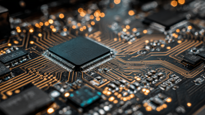
Printed Circuit Boards, or PCBs, are essential components in modern electronics. These boards serve as the backbone for countless devices, from smartphones to home appliances. A Printed Circuit Board is not just a flat piece of material; it is a complex assembly of pathways and connections that facilitate the flow of electricity.
Understanding how a PCB works requires diving into its structure. Each layer is intricately designed with copper traces that form electrical circuits. This design reduces the need for bulky wiring, streamlining production and improving efficiency. However, creating a flawless PCB is a challenging task. Imperfections in design can lead to circuit failures. Engineers must constantly refine their techniques to overcome these hurdles and improve reliability.
Furthermore, the rapid evolution of technology pushes the limits of PCB design. New materials and methods emerge regularly. Yet, with innovation comes the risk of creating problematic prototypes. As we explore what a Printed Circuit Board truly is, it becomes clear that while these boards seem straightforward, they encompass a world of complexity and constant improvement.
What is a Printed Circuit Board (PCB)?
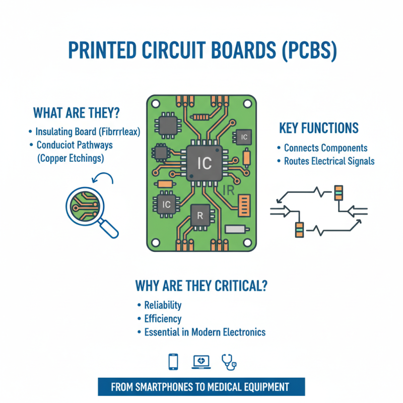
A Printed Circuit Board (PCB) is a fundamental component of modern electronics. It serves as a substrate to connect different electronic components like resistors, capacitors, and microchips. Typically, a PCB is made from insulating materials, such as fiberglass, with conductive pathways etched into the surface. These pathways allow electrical signals to pass between components, enabling the device to function properly.
PCBs can vary in complexity. Some are simple, with only a few components, while others may have multiple layers and hundreds of parts. The design process is critical. Even small mistakes can lead to malfunction. Engineers use specialized software to create designs, but errors can occur, leading to failed prototypes. Tests are essential to identify these flaws.
The manufacturing process involves several steps, including etching, soldering, and assembly. Each step carries its own risks. Improper soldering can cause short circuits, while etching may not always produce clear pathways. Engineers must continuously review and refine their designs to prevent these problems. Being meticulous is key. In the end, the effectiveness of a PCB greatly affects the overall performance of an electronic device.
What is a Printed Circuit Board and How Does it Work?
| Feature |
Description |
Function |
| Conductive Pathways |
Copper traces that connect different components. |
Facilitate electrical connections. |
| Components |
Electronic components such as resistors, capacitors, and microchips. |
Perform various electrical functions. |
| Substrate |
Base material that supports components and circuits, often fiberglass. |
Provides structural integrity. |
| Solder Mask |
Protective layer that prevents solder from bridging between conductors. |
Ensures proper soldering and prevents shorts. |
| Silkscreen |
Printed labels and markings on the PCB for identification. |
Helps in assembly and troubleshooting. |
Key Components of a Printed Circuit Board
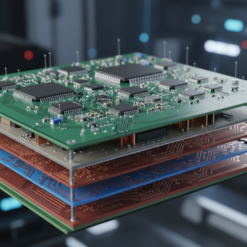
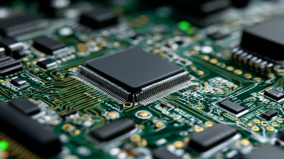
Printed Circuit Boards (PCBs) are essential in modern electronics. They consist of a thin board of insulating material, like fiberglass, with conductive pathways etched into their surface. These pathways connect various components, allowing electrical signals to flow. The reliability and efficiency of PCBs make them critical in devices ranging from smartphones to medical equipment.
Key components make up a PCB. The most fundamental is the substrate, which provides structural support. Copper traces form the circuitry, guiding electrical flow. Solder pads allow components to be securely attached. Capacitors and resistors regulate power and control signals. According to industry reports, PCBs account for about 10% of the total cost of electronic devices, emphasizing their importance.
However, the PCB manufacturing process can be problematic. Issues like misalignment of components during assembly can cause failures. Environmental concerns arise too; the production and disposal of PCBs can generate toxic waste. This challenges manufacturers to innovate sustainably. As the demand for electronics grows, so does the need for efficient, environmentally friendly PCB solutions.
The Manufacturing Process of PCBs
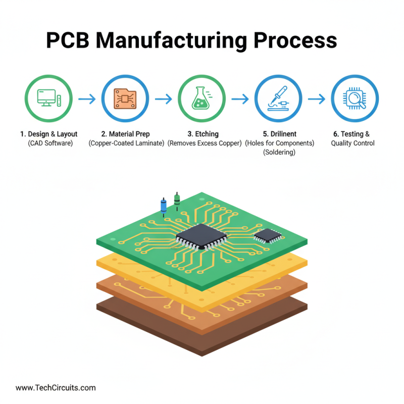
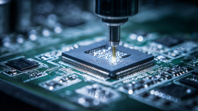
The manufacturing process of printed circuit boards (PCBs) involves several detailed steps. Initially, a design is created, usually using specialized software. This design includes the layout of electrical pathways and the placement of components. After finalizing the design, it is transferred onto a copper-coated laminate. The laminate is then subjected to a series of etching processes, which remove excess copper and reveal the circuit patterns.
Next, holes are drilled to allow for component placement and interconnections. This is a critical phase, as precision is crucial. Any misalignment can lead to functional failures. After drilling, a plating process applies a thin layer of metal to the holes, ensuring good electrical connections. Following plating, a solder mask is applied. This layer protects the circuit from environmental damage, but it can sometimes complicate soldering.
Finally, the boards undergo inspection and testing. Automated systems check for defects, but human oversight is still necessary. Some boards may pass visual inspection yet fail in functionality. There are always areas for improvement in the manufacturing process. Even small errors can lead to significant issues later on. Each step requires careful monitoring, and constant refinement is vital to achieving high-quality results.
How Printed Circuit Boards Function in Electronic Devices
Printed circuit boards (PCBs) are essential components of electronic devices. They connect different electronic parts, allowing them to work together. The pathways on a PCB create a circuit, which allows electricity to flow. This flow is crucial for the device to function correctly.
In smartphones, PCBs are compact and intricate. They can fit in small spaces yet accomplish complex tasks. A PCB might support processors, memory chips, and sensors all at once. Each component relies on these connections to relay information accurately. A poor PCB design can lead to device failure. Researching and testing are vital for effective PCB design.
Tip: When designing a PCB, consider space optimization. A cluttered board can complicate assembly and repairs. Simplicity is often more effective.
Another aspect of PCBs is heat management. Excess heat can damage components. In designing your circuit, think about heat dissipation. You might need to add heat sinks or ventilation paths. This can prolong the life of your electronic device.
Tip: Regularly test your PCB prototypes. Early mistakes can lead to costly issues later. Learning from these mistakes helps in improving future designs. Working with PCBs requires attention to detail and constant reflection on the design process.
Common Applications of Printed Circuit Boards
Printed Circuit Boards (PCBs) are essential components in modern electronics. They are used in various devices, from smartphones to cars. In each device, the PCB acts as a foundation connecting electronic components. They shape how signals travel and power flows.
PCBs are found in countless applications. For example, in consumer electronics, they help manage signals in televisions and game consoles. In healthcare, they control devices like heart monitors and imaging machines. They even play a role in renewable energy systems, such as solar inverters. However, some designs can be overly complex and hard to troubleshoot, causing inefficiencies.
In the automotive industry, PCBs contribute to functions like dashboard displays and safety systems. Yet, they can also create challenges. If not designed properly, they may lead to failures. This highlights the necessity for careful planning and testing. Each application varies in requirements, reflecting the diverse landscape of technology today.
Common Applications of Printed Circuit Boards (PCBs)


 Phone
Phone WhatsApp
 Email
Email

